|
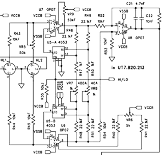
Here's an excerpt from the circuit
diagram, showing the two Hall sensors
HL1 and HL2 (the round things on the left) and their related
conditioning electronics. The output of the U8 op-amp (top right,
wired as a differential amplifier) is the analog signal of interest.
The range switching is handled by two sections of U5 (the
boxy things), which is a CMOS 4053 (triple
2-channel analog mux) in the feedback path of op-amps U6 and
U7 (output amplifiers for the two Hall sensors), and chooses
between two sets of feedback resistors (whose values in the schematic are
wrong, by the way—both the 40 A and the 400 A ranges
seem to have identical feedback resistor networks, which obviously
can't be correct).
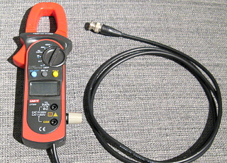
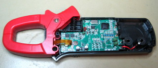
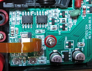
However, I hit an unexpected snag when I opened up my UT203—mine
seems to be a newer revision, with a different circuit. The PCB on mine
is labeled "UT203/204 REV.3 2018.08.15", and at the very
least it:
- has different op-amps (two GS8552 rail-to-rail low-voltage
dual op-amps, whereas the schematic has OP07 single
op-amps)
- has no 4053 (unless it's on the reverse side of the board,
which I did not remove for inspection)
- has a 24LC04B eeprom chip, for whatever reason (factory
calibration data, I'd guess)
- seems to have a different central IC as well, at least based on its
pin count.
Nevertheless, I think the analog front end of the Hall sensor read-out
circuit must be essentially the same as what is shown in the schematic.
I just need to find the correct pin on the correct op-amp to get the
output signal I want.
|
|
So I looked up the
datasheet for
the GS8552, and armed with its
pinout, I switched the instrument on and began probing the two op-amps
IC6 and IC7 with a multimeter, measuring against the COM
terminal of the UT203 (which was just a lucky guess as to what
might serve as "ground"). I first measured the supply voltages.
Then I measured each output pin with zero current, +4 A current, and
−4 A current passing through the clamp. (At this time I paid
no attention to whether the wire is properly centered and perpendicular
to the clamp, as it should be for accurate results.) I observed that:
- on either amps range, both op-amps are fed with +1.95 V (Vdd)
and −1.09 V (Vss). The battery
terminals, at the same time, measure +7.99 V and
−1.09 V relative to COM.
- on the volts and ohms ranges, the op-amps are still powered,
being fed with +1.11 V and −1.82 V, whereas the battery
terminals are +7.51 V and −1.82 V.
- on the Hz range, battery negative measures −1.46 V, and
on the diode test range −0.37 V.
- on the 40 A range, the outputs A and B (pins 1
and 7) of IC6 and IC7 measured:
| No current |
+4 A current |
−4 A current |
| IC6 output A |
−164 mV | −176 mV |
−155 mV |
| IC6 output B |
−164 mV | −155 mV |
−172 mV |
| IC7 output A |
+263 mV | +262 mV |
+264 mV |
| IC7 output B |
−2 mV | +21 mV |
−18 mV |
So it seems like COM is at a virtual ground that is adjusted
differently for different measurement ranges. On the amps ranges it
is some 1.09 V above the battery negative terminal, and on other
ranges within reasonable (and safe) limits not to wreak havoc with any
op-amp I choose to use. The two op-amp
ICs seem to be powered through a 3 V regulator, likely IC3
which is marked "SD30L".
The two halves of IC6
seem to do the job of op-amps U6 and U7 in the old
schematic, i.e. they amplify the Hall sensors' outputs—note
how they act as "mirror images" of each other with positive
and negative current through the clamp. The
"B" half of IC7 seems to be the differential
amplifier (U8 in the old schematic) and its output is the analog
signal that's proportional to the measured current. Its output
is very close to 0 V at zero current, which confirms that the
COM terminal is indeed at the correct virtual ground here. The
"A" half of IC7 is probably the constant-current
supply for the Hall sensors, as it never changes at all.
|
|
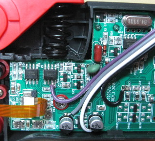
To connect my own circuit to the instrument, I needed access not only to the
analog signal from IC7, but also to the virtual ground, and
on/off-switched power supply voltages (VccB and VssB in the old schematic).
I did not want to remove the
circuit board in order not to disturb the connections to the buttons and
LCD (sometimes reassembly can be a pain, so I try to minimize disassembly).
Therefore I chose locations that are easily accessible to the soldering
iron on the front side of the PCB:
| VccB | positive leg of C16 (gray) |
| VssB | negative leg of C14 (white) |
| GND | upper end of LC1 (black) |
| Signal | pin 7 of IC7
(purple) |
I breadboarded a circuit using an
LM358 op-amp and started testing. I chose the LM358 just
because I happened to have it immediately
available in shelf. It is unity-gain stable, and its input and output
voltage ranges go within
20 mV of the negative rail, so it will work just fine with a
virtual ground 1.09 V above negative rail. The positive end of its
output range is more limited, some 2 V below the positive rail,
but that's ok as I'm
using the unregulated battery voltage, not the regulated 3 V, as the
LM358's positive rail. The output range (which needs to be symmetric)
is, of course, limited by the negative supply to ±1 V, but
if I aim for 10 mV/A sensitivity (the same as on the
Fluke i310S), the full-scale output will be just
±0.4 V, which is ok.
|
|
With wires soldered so I don't have to hand-hold the multimeter probe,
I was able to more carefully measure the analog voltage with respect to
current, this time with the wire properly positioned in the current clamp's
jaw (not that it seems to matter much). The analog signal from IC7
turns out to be 6.53 mV/A on the 40 A range, and 0.638 mV/A
on the 400 A range. (Rather strange values, but if the
instrument is factory calibrated into the eeprom chip, the exact magnitude
of the analog signal doesn't really matter. However, if you do the same
modification on your own instrument, you'll likely get different values, and
will need a different gain—probably the gain potentiometer in my circuit
will accommodate it, though.)
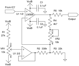
The output circuit I designed could
hardly be simpler—it is just a non-inverting amplifier (with
gain that can be set with trimmer VR2 from about 1.2× to
1.7× to get the desired 10 mV/A sensitivity) with an offset
control. Note that the analog output's offset is not affected by the
instrument's own zeroing function, and likewise the digital readout is
unaffected by the offset potentiometer—the two are completely
independent. The voltage from the divider formed by R1 and
VR1 is about ±1 V relative to the virtual ground. That
becomes about ±60 mV in the following voltage divider formed by
R2 and R3. The impedance of that divider is about
20.6 kΩ,
and together with R4 and VR2, the feedback network gives the
upper half of op-amp U1 the desired gain range. Note that the input
signal connects to the op-amp positive input only—that input is
high-impedance, so my circuit does not load the signal in any significant
way, and should therefore not affect
the internal workings of the UT203 at all. Also, since no feedback
resistors connect to the input signal, there's no way that my circuit,
which runs off a higher voltage, could damage the low-voltage IC7.
Since the offset voltage is derived directly from
the unregulated battery voltage, it will drift slightly as the battery
wears down, but that's not really a big deal compared to other drifting
in a cheap instrument like this.
The output impedance of my circuit is 10 kΩ, which is high enough to
make an inadvertent short-circuit a non-issue, yet low enough not to skew
the voltage at an oscilloscope's input, which is typically around
1 MΩ.
|
|
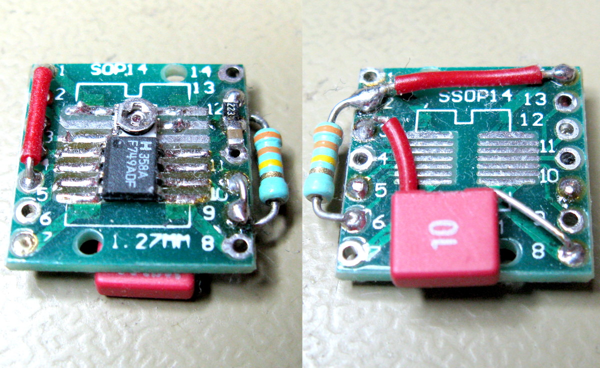
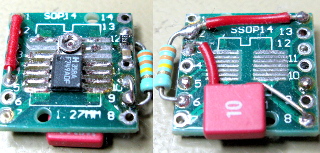
There's plenty of room inside the instrument's case otherwise, but the
populated circuit board cannot be very thick. A DIP op-amp on a scrap
of veroboard might just fit, but since I had SMD components
handy, I played it safe and used those as much as possible. I built the
circuit on a tiny 14-pin SOIC-to-DIP adapter PCB from eBay—the IC
and gain trimmer fit nicely on the SOIC pads, and the two capacitors and
five resistors, in either SMD or through-hole format, go between various
DIP pin holes. A custom PCB might look better, but with such a simple
circuit I just couldn't be bothered to fabricate one.
Here is a bigger photo of this mess.
|
|
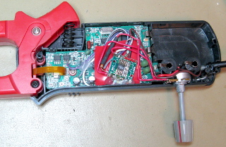
I stuck a couple of layers of electrical tape (bush-league though that is)
over a suitable part of the instrument's PCB for insulation, and wired up
my own PCB to sit there, with the trimmer (gain) potentiometer side facing
up. Some hot glue keeps it from wandering about. Once the instrument's
case is closed, it should be quite snug in there.
The offset adjustment potentiometer is located near the banana jacks,
where a small pot (4 mm shaft) will just fit after some
grinding, but this was the tightest and most awkward bit of the whole
modification. The output cable exits the instrument through a hole I
ground near the lanyard
attachment point, at the lower-right corner of the case. A cable tie
provides strain relief. The coax shield is connected to the virtual ground
at the COM jack. Click
here for a bigger photo.
I adjusted the gain potentiometer by feeding 10 A current through
the jaw (I looped a wire through it five times, centered it as carefully
as I could, and fed it 2 A from my power supply), while
monitoring the output on my oscilloscope. After that I reassembled the
instrument's case and cut the offset potentiometer's shaft to its final
length.
|
|
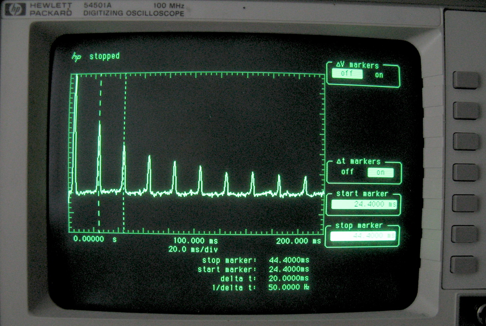
The thing works as intended, though it's quite sensitive to external
interference. Adding some copper tape inside the case, grounded to the
negative terminal of the battery, improved it somewhat. It still helps to
switch off the fluorescent ring light in my desk magnifier lamp when using
this with the oscilloscope, big deal. Or I can put multiple turns through
the jaw to get more signal, and scale the results accordingly. It's accurate
enough on the 40 A range (well, I calibrated it, didn't I), and the
400 A range doesn't seem to be too far off either.
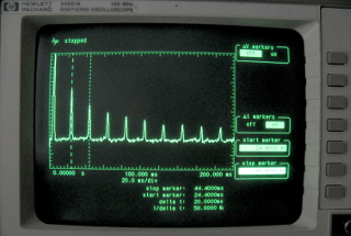
Here's an example oscilloscope
trace of the inrush current when switching on my 200 VA isolation
transformer. The first peak is some 120 mV, which would be 12 A,
but I had four turns through the jaw, so it comes to 3 A. The
peaks occur at 20 ms intervals (that's 50 Hz), and the peaks
are all either positive or negative, depending on the magnetization state
of the transformer's core when it was last switched off, i.e. during
which half-cycle of mains AC power. As there was no load connected, no
current flowed after the initial inrush.
|
|
As these clamps are mostly used to measure things like household AC current,
I wouldn't be surprised if the instrument's bandwidth were just a few
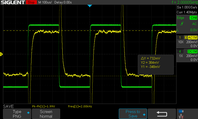
hundred Hz. To gain some idea of the bandwidth, I fed an ordinary stereo
amplifier with a sinewave from my signal generator, and connected an
8 Ω power resistor to one of the speaker outputs. I then looped
the output wire through the clamp's jaw a couple of times, and increased
volume, while monitoring the output on my scope. I set the cursors at the
sine wave's peaks at 500 Hz, then started increasing the frequency.
The output amplitude stayed very constant up until 2 kHz, but beyond
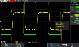
that it, surprisingly, began to increase. I switched to a
square wave, and saw this waveform
(the green trace is the input signal, the yellow trace is the current
clamp's output). Obviously something causes a tremendous high-frequency
response somewhere,
and I don't really know whether it's in the stereo amp or in the current
clamp. But at least up to 2 kHz the thing behaves very well.
|
I don't know if the same modification is
applicable to the
Of course, I take no responsibility for the correctness of the above
information, and if you decide to modify your own current clamp, you do so
entirely at your own risk. Let me know how it turns out.