<HOME
<Test equipment
<Electronics
<Workshop stuff
My home made UV light box for exposing photosensitive PCBs
|
While I mostly build my one-off electronic projects on Veroboard or
similar, proper PCBs are sometimes necessary, and not all that hard to
make at home—especially single-sided ones. After drawing the
layout, I find the most tedious chore is
drilling holes for through-hole
components—and even that can be avoided by using surface-mount
devices.
I use ready-made photosensitive PCB material, which I expose
through two laser-printed transparencies (you know, those used with an
overhead
projector—or are you too young ever to have used one?)
carefully aligned and taped together (a single print will have too
many holes in it). Over them I place a sheet of glass (I have
somewhere an old semiconductor photomask stripped clean of its
emulsion, but ordinary glass taken from a photo frame does work just
as well, and is more readily available) to press the transparencies
against the PCB. I expose them, develop with suitably diluted drain
opener (no need to buy pure NaOH pellets, which are hugely more
expensive), etch with sodium persulfate (or hydrochloric acid with
hydrogen peroxide, or diluted nitric acid, or whatever I have
available), and strip with acetone. When using trough-hole components,
I drill the board with my Porxxon mini drill
which is mounted on a drill stand. To make alignment easier, I've added
a USB microscope to the drill stand,
With an adjustable crosshair
overlay I can see exactly where the drill bit will hit the PCB.
Sometimes I will even tin the copper areas.
Last time I needed a custom PCB, I finally went ahead and built myself
a proper UV exposure tool, as
described here. The PCB fabrication process is
described further down.
|  |

|
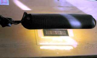
I used to do the exposure with
an ordinary fluorescent tube desk
lamp, which produces enough UV (or almost-UV) to expose a small board
in some 20–30 minutes at close distance (larger boards need
the light to be further away to illuminate the whole board, or moved
regularly along the length of the board, so the time is
correspondingly longer). That was convenient enough, as the lamp was
right there whenever needed, and I rarely was in any hurry—but
you can't get the environmentally disasterous mercury-laden tubes
anymore (regardless how "green"
CFLs
were touted as, while transitioning away from incandescents)!
But, surprisingly, I found you can still get compact fluorescent
"blacklight"
bulbs for your home discotheque. (Well, you could way back in 2024
anyway. And I'm not sure, perhaps these also have been outlawed, but the
store was allowed to sell its remaining stock? So if you can't get them
either, you'll be looking for an LED-based solution.) So I bought one
of those, and built a dedicated,
"real" UV exposure box to house it in. With my extremely
infrequent use, the bulb should last forever, plus I bought a spare one
as well. (And while laser-printable
transparencies are still available, I also stocked up on those! Expect
them to finally disappear from stores any day now!)
|

|
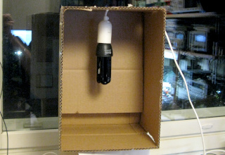
Instructions on the Net say you need
a cardboard box and a suitable
lamp holder and power cord. Hang the UV bulb in the box, place the PCB
underneath, and expose away!
Awful.
I mean, it will probably work just fine, but when doing anything, why
not overdo it? Why not go absolutely overboard with the
design? I happened to have some thin aluminum sheet metal
in-shelf to make a reflector of sorts, so as I I bought the UV bulb,
on a whim I picked up a piece of plywood as well (actually an extra
shelf for a cabinet of some kind... I've later used three of the exact
same shelves to build a dust containment
tub for my Proxxon mini drill setup).
In one evening, I built a
much nicer exposure box. Good and sturdy, no wobbly cardboard, it sits
properly above the PCB and will certainly give more uniform and
consistent exposures!
|

|
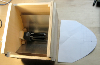
Here is a photo of the box
upside down, looking into the reflector. The two plywood pieces on the
left and right have grooves milled into them, which hold the aluminum
reflector in place (and in shape). The left-hand one also has a hole for
the lamp holder, roughly at the reflector's focus. Some extra support is
provided by six bits of square(ish) wooden dowel, three on either side
of the plywood, glued on with epoxy (you can see the inside three
surrounding the base of the bulb in
the photo). I didn't bother
attaching the lamp holder any more permanently, so it will just slide
out if the bulb is first removed.
The design process was very scientific: I plotted a couple of
parabolae, and eyeballed one of suitable
dimensions. :) The manufacturing process was highly
technical as well: I printed out the parabola, cut the paper
along the curve, and traced its edge with a pen onto the two pieces of
plywood. (The paper stencil is in the photo on the right.) Using a
2 mm wide milling bit with
my Proxxon IBS/E in
its MB-200 stand, I hand-fed the plywood along the curve and
managed to cut reasonable grooves some 6 mm deep into the
10 mm plywood. I bent the aluminum into roughly the same shape,
and had little trouble fitting it into the grooves. The two other sides of
the box (upper and lower in the photo) came from the same scrap of
plywood, and attached with wood screws to the two others. (Sorry I
didn't think of taking photos during assembly, but you can probably
see what I've done from the
finished product.)
|

|
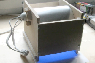
This is how the box stands on
the desk. The appropriately masked PCB goes underneath it. The bulb is
some 13 cm above the surface of the desk, and there are slots at
the bottom of the box and at the sides of the reflector to allow air
circulation. (Actually, the bottom slots were dictated by the size of the
leftover plywood, after I had cut the first two pieces to hold the
reflector.) Whereas the 15 W bulb heats the aluminum reflector
to somewhat over 40°C, the PCB being exposed remains pretty much
at room temperature.
The standard E27 lamp holder protrudes from the left-hand side of the
box, and has an on/off switch in its cord. You can see the three
support pieces placed around it, just like inside the box, in the
photo. (The
"extra" piece of square dowel along the lower edge of the
left-hand side has no purpose here—it was part of the shelf I
sourced the plywood from, and I just didn't bother to remove it. )
|

|
The bulb's actual tubes are about 80 mm long, and at the distance
that they are, the 100 mm wide PCB ought to be pretty uniformly
illuminated along its entire width. With the reflector, the
illumination seems visually very uniform in the perpendicular
direction as well; I'd be surprised if it couldn't expose the whole
160 mm long PCB in one go. (Not that I fabricate such large PCBs
very often. The first PCB I used this device on was just
20×30 mm—though I did make four of them at once, so
80×30 mm then.
But on the few instances that I have exposed a whole 160×100 mm
using a desk lamp, I've shifted the lamp along the board's 160 mm
length several times during quite a long exposure.)
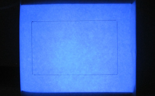
Here's a photo of the box on
its side (with the UV bulb vertical), with a blank paper fluorescing in
front of it. The rectangle drawn on the paper is the size of a
100×160 mm PCB. (And here
is a professional-grade schematic of where the ultraviolet CFL bulb and
its holder are behind the paper, and what their relative sizes are.)
Not bad, huh? According to Gimp's color picker tool, the
bright central parts seem to be only some 20% brighter (on a linear
scale) than the darkest corners of the rectangle area. The required
exposure dose for the PCB is certainly less critical than that!
|
The process
I'm using up my >10 years old PCBs first (have I really gone
that long using just Veroboard???). They still work sorta-kinda
ok, only their peel-off backing leaves some black goop around the edges
of the board—that adhesive seems to degrade faster than the
photoresist! However, fresh boards will likely do with a much shorter
exposure time. I'll update that here once I get around to it, but here's my
recipe for these long ago expired boards:

|
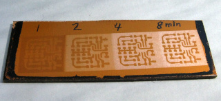
- Expose 10 minutes with the 15 W bulb. In an
exposure time test, 4 minutes
already looked very good, but 8 minutes resulted in just
perceptibly less residues. In another test, there was no further difference
between 8 minutes and 16 minutes. I tried etching the 4 min
and 8 min test PCBs, and the 4 min was no good, but
the 8 min was pretty ok, considering the age of the PCB material!
So I settled on 10 min exposure time, just to play it safe.
If I were trying to make ultimately narrow traces, where exposure
time might be more critical, I'd certainly use a fresh PCB, not one
with a decade old expiry date! :)
- Develop 1+ minute with agitation in domestic Pirkka
Putkenavaaja drain opener solution, diluted with water to 1/10
of its original concentration. I think Pirkka is at the milder
end of the NaOH concentration
range, judging by its density; other brands of drain opener will
likely need to be diluted more. About 1% NaOH by weight should
be a reasonable concentration to aim for, if the concentration
happens to be specified on the bottle.
|
Pro tip: Underexposure can rarely be adequately compensated with
overdevelopment, so it's better to err on the side of overexposure,
and to develop only as long as visually seems necessary! The same goes
for overetching:
Unless there's serious photoresist residues remaining on the PCB due to
underexposure, underdevelopment or over-aged boards, the etching time should
be quite independent of the above. But any residues that do hinder etching
are unlikely to be helped much by overetching the board. Instead, the traces
will just get narrower and narrower.

|
- Etch 10+ minutes with agitation in a solution of
20 g sodium persulfate for every 100 ml of water. Use as
hot water as you can get from your faucet (usually that's about
60°C). The etch rate will go down as the solution
cools(*), so
especially with small etchant volumes (for small PCBs), you may need
to carefully heat up the solution in a microwave halfway through. (Take
the PCB out first, and don't go anywhere near boiling!)
- Once the board begins to look good, overetch it for a while to make sure
you leave no short circuits anywhere. Then rinse it off and inspect it
under a magnifier, and etch some more if necessary.
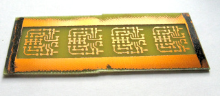
Unlike above, where I tested four different exposure times, this is a
"production batch" of four PCBs at once. (There's no sense in
making only a single one of such a tiny board—the saving is
minuscle, and either I'll mess up the first prototype
and need another PCB, or I'll find use for another one later, or
someone else will become interested and request a PCB!)
The edges of the traces are all
ragged and "fuzzy" with these
over-aged PCBs, so for anything more demanding than a SOIC (at 1.27 mm
pitch) I'd absolutely use a fresh board instead!
|
(*) A chemists' rule of thumb says the reaction rate will
approximately halve for every 10°C reduction in temperature. So if etching
takes 10 minutes at 60°C, expect to etch almost three hours
at room temperature!
The reaction between the persulfate ion and copper is:
Cu + S2O42- →
Cu2+ + 2 SO42-
and from their molar masses you can calculate that a gram of sodium
persulfate will etch 0.27 g of copper, or 0.030 cm3,
which is about 8.5 cm2 surface area on a single-sided PCB
with the typical 35 μm copper. 20 g of sodium persulfate in
100 ml of water, per the above recipe, should therefore be
just sufficient to etch an entire 160×100 mm PCB completely,
especially if you make copper fills in any large unpopulated areas, rather
than etching them completely free of copper. However, 100 ml is a
dismally small volume of liquid to spread over a PCB that size. The
liquid would only be some 6 mm deep—and even shallower, if you
etch in a pan any bigger than the PCB! So go ahead and mix up a sufficient
amount of solution, some 300–400 ml at least for a PCB that size,
and then you can also rest easy knowing the etchant won't run out of
oomph halfway through the copper. After all, the
etch rate will also decrease with decreasing etchant concentration, not just
with decreasing temperature!

|
After etching, wipe the board free of the photoresist, first with acetone,
then with isopropyl alcohol. Then, if you're using any through-hole
components, drill the board.
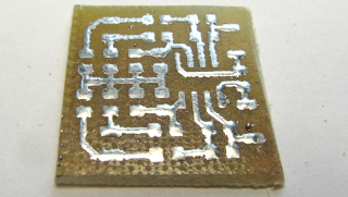
Finally, if you like, you can tin the board by
applying Bera-Fix solder tinning compound with a cotton bud, and melting
it with a heat gun. (Or you can spread flux over the board, and trace all
copper areas with a bead of molten solder on the tip of your soldering
iron.) Then scrub away the flux residues and loose solder
beads with acetone again, and finally with isopropanol. Inspect the
result carefully—there's still solder beads and residues visible
in the photo, demanding more
scrubbing! The solder plating also looks needlessly thick, I guess I was
a bit too liberal with the Bera-Fix this time.
The PCB is for a two-channel balanced to unbalanced audio converter, which
comprises a dual op-amp and a bunch of resistors and capacitors. I made it
in SMD only because the end application didn't have much room inside. (Ok,
I made it in SMD because I was too lazy to drill holes. Happy now?) It
went into a mixer whose AUX RETURN inputs were, for some unfathomable reason,
unbalanced!
|
Radiation, electrical and chemical hazard warning!
Please be aware that UV bulbs, though they may be sold even for
recreational use at home, may present a significant hazard to
eyesight! Do not stare into the bulb under any circumstances,
and do not assume that the bulb will only emit the supposedly
less-harmful "UV-A" radiation! There are numerous documented
instances of cheap Chinese UV bulbs blasting out significant amounts
of the more harmful UV-B (or even UV-C?), with party guests suffering
eye or even skin problems the following day! Put the bulb in a box
where you can't at least see it directly, and do avoid staring into
direct reflections as well!
Also, don't make the household AC-powered lighting fixture yourself,
if you're at all uncertain of how to do it properly! I'm sure you can
scavenge a bulb holder, cord and switch already wired up and ready to
go from some cheap ready-made lighting appliance at your local
hardware or home furnishing store such as Ikea.
Finally, wear appropriate hand and eye protection when handling the
chemicals for developing, etching and stripping your PCBs! Drain
opener (sodium hydroxide, a.k.a. lye) is especially hazardous
for your eyes—a single drop can actually blind you! (It's
astonishing that the stuff is sold in supermarkets, yet half our
population isn't blind already!) And your skin will absolutely not
appreciate the highly oxidizing and/or acidic copper etchants, nor the
acetone, for that matter (despite it being commonly used as nail
polish remover)! These substances will also have cumulative
effects, just in case the first contact doesn't kill you
sufficiently. And dispose of used solutions
appropriately—dissolved copper is a toxic heavy metal, you know,
right? Right??? You see, I'm actually a chemist by training,
but I foresee a greater than 50% probability that you're not! If
nothing else, at least wear goggles, for fsck's
sake!!!
So do this at your own risk, and don't blame me for anything
bad that happens!
Antti J. Niskanen <uuki@iki.fi>
